
Services
The Handling and Processing of Semiconductor Wafers
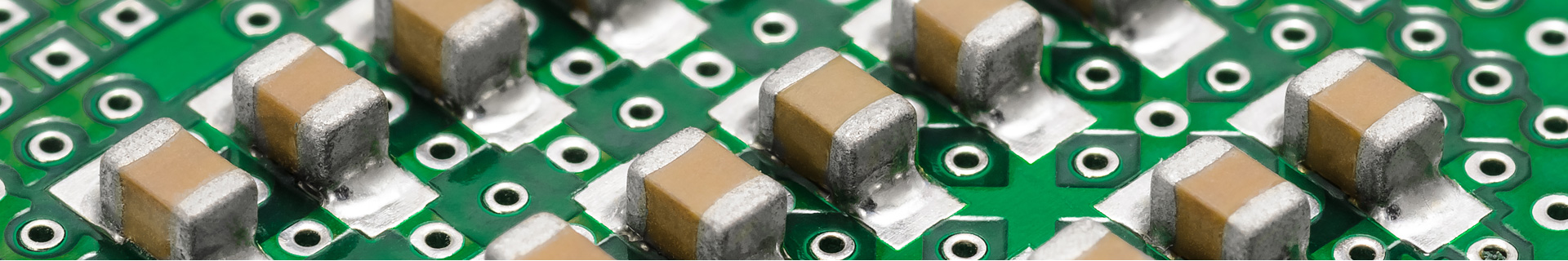
SemiDice has been processing silicon wafers from the industry’s leading semiconductor manufacturers for over three decades. We have the capability of processing wafer sizes up to 8″, including custom wafers with multiple die sizes on a wafer. We can halve, quarter or singulate wafers. Whether it’s a single wafer, or several hundred, Semi Dice can process silicon in a timely fashion.
Contact a SemiDice salesperson who can discuss with you your requirements at (800) 345-6633.
The following outline will show the process from incoming inspection through finished product for inventory. This is a general overview and will not include the many intricate details we address and multitude of steps that need to be taken throughout the process. If you wish to learn more about our processing flow and have questions, please contact a Semi Dice salesperson.
I. Introduction
The biggest concern of semiconductor manufacturers, Semi Dice and bare die end-users is to ensure the fragile material is handled properly. From initial receipt through processing and final shipment, EDS (electrostatic discharge) and contamination precautions are requirements that cannot be overlooked. In-depth training for our employees is critical so the proper handling of the product takes place.
II. Precautions
ESD ~ Contamination ~ Audits
The voltage potential of the human body is generally considered the most common cause of ESD induced damage. Lab tests have shown that as few as 100 volts can severely stress GaAs FETS, MOSFETS and virtually destroy EPROM’s. It is not uncommon for a person to develop a static discharge as high as 15000 volts. In low humidity, a person walking across a carpet can build up as much as 35000 volts with respect to the ground. (Mamoon Rashid – 1995 article ESD & the Fragile IC). Our work stations have the necessary devices and safe guards in place to protect from ESD damage.
Static dissipative table mats, station ionizers, continuous wrist strap monitors, special flooring, cleaning solutions and garments all assist in the protective area control. Semi Dice performs a regular check of our grounding system, which includes a visual verification of earth ground and a spot check with a continuity meter. Each table mat is checked for resistance to ground and resistivity.
ESD damage may be visible after the device has been mounted into a circuit and power applied. Temperature and humidity levels need to be monitored. This is accomplished by set time checks, or continual monitoring. Although temperature is strictly a human comfort issue, humidity directly affects product. Humidity levels to high can adversely affect the product by air borne contamination deposits, where as low humidity levels will add to the static generated, with potential damage to product at handling.
Regularly scheduled particle counts with absolute and control limits are in place and conducted to control contamination. These counts are performed at work stations and various identified locations within our clean rooms.
Contracting to an outside service dictates the explanation of the operations performed within the area to insure the potential for product contamination is minimized. Specialized garments such as lab coats or “bunny suits”, booties and bouffant cap or hoods and face masks are just a few of the utilized items for our clean room attire.
Our quality program includes regularly scheduled audits for ESD and clean room contamination.
III. Product Inspection
Product Inspection ~ Product Movement
Semi Dice receives both individual die and silicon wafers. Product is inspected at incoming for proper packaging from a supplier or customer to insure ESD and contamination protection are met. Supplier product visual and dimension inspections are done to insure product compliance. Customer supplied material is checked in the fashion.
Tyvek is the preferred insert at Semi Dice. Once product has been accepted, it needs to be moved for processing or to inventory. Product movement should take place with ESD and contamination controls in place. Faraday cage shielded bags, carriers or metal pans are acceptable means for product movement.
IV. Wafer Mount
All bare die starts off in wafer form and must be sawn into individual dice. Proper handling of a wafer dictates again that ESD and contamination procedures are in place.
Wafers are mounted on a tape frame at a grounded work station with the operator wearing a wrist strap.
V. Wafer Saw
Die Separation ~ Loading
Wafer sawing is performed using de-ionized water. At Semi Dice, the water resistivity is continually monitored by use of a wall mounted resistivity meter. We typically run our water at a 18 megaohm level for resistivity, with 16 megaohms minimum set as our control, with an absolute of 15 megaohm limit. The ultraviolet lamp indicator and filters are changed by the DI water maintenance service as required. The water is analyzed for; total organic carbon, bacteria count, total dissolved silica, particulates and residue. ESD precautions, water contamination controls and resistivity measurements minimize the migration of contaminates and silicon dust on the wafer surface.
Depending on the size of a wafer, the quantity of good die per wafer can range from less than 100 pieces to 80,000 pcs.
The sawn wafer is then moved to the next operation of die removal from the tape or frame. Typically a demounter, or automatic pick and place machine is used for separation. This has proven to be the most cost effective and “die friendly” method, since product is removed from the nitto tape separating the devices with minimal contact between the die. Again, the individual operator performing the loading step is wearing their wrist strap and working at a formal loading grounded station within the clean room environment.
Our preferred manual loading tool is a vacuum pencil with pick up tip that accommodates the die size with minimal contact. Teflon, plastic and rubber tips are all acceptable materials. Product is picked up with a vacuum pencil from the corner or side of the die. Large devices (200 X 200) normally use a rubber tip with the pick-up from the top surface for loading.
Automated equipment may include a pick-and-place machine that removes die from the tape. A video screen will allow the operator to position the pick up collet over the center of the die. A needle(s) pushes up from the back and dislodges the die from the tape. The vacuum collet then lifts the die from the tape and places it into the carrier. This method is preferred for Gel-Pak carriers since it produces consistent alignment of die. Manual loading does not allow to this accurate placement and pressure of die onto the membrane.
Proper handling of the bare die at the load operator is critical to the life of the die. Mishandling could inflict scratches, chips, cracking and contamination being transferred to the die. Working without proper ESD measures in place could cause latent electrical defects.
VI. Packaging
Carriers ~ inserts ~ lids ~ visual
After the die is separated it is loaded in chip carriers called waffle packs. The carriers have cavities that the die is placed into. The cavity size is determined by die dimensions (length, width and thickness) and is important to die safety. Die supplied in a cavity that is too large allow the chip to rotate or flip. Proper carriers will minimize die movement, yet permit ease of placement and die removal.
Lids are key in maintaining die placement. Dimpled lids are used for thinner devices because they assist in holding the insert to the top of the carrier surface, minimizing die movement within the cavity. Flat lids are used when the die height is just below the carrier surface. There is no additional pressure when the insert is added and the lid is placed. A flat lid may require two or more inserts to ensure the devices remain within the cavity.
Semi Dice utilizes three types of inserts; uncoated rice paper, Tyvek and silver saver. Our preferred insert is Tyvek. This is due to the ESD and environmental precautions.
Rice paper is an acceptable insert, however product tend to stick to the rice paper and usually causes displaced product once a carrier is open. We use silver saver inserts for product that is susceptible to corrosion or tarnishing.
Product is then moved to the visual inspection operation. Again the inspectors are working within the clean room environment, wearing their ground strap at a formal grounded station. The operator has available many of the same tools utilized at the load operation. The vacuum pencil and tips are used for the removal of discrepant product.
VII. Storage
Dry Boxes ~ Environmental Concerns (humidity) ~ Audits
Once product has completed its cycle through saw, load and visual operations, storage is the next area of concern. Most devices and many metal compositions are susceptible to the environmental concern of moisture. Product with silver back metal or bond pads if not sorted properly, over time, experience metal corrosion or tarnish. This can result in adhesion or bondability issues.
Product is protected within the clean room, using ESD precautions with minimal exposure to contaminants and is then stored in a dry box. The typical dry box is a plexiglass container filled with a continuous flow of nitrogen, as well as tight door seals insuring the inner atmosphere remains inert. Routinely monitoring nitrogen flow, humidity indicators and regular inventory audits, insure that the product has not started to degrade as well as insuring contamination has not been introduced.
Conclusion
Handling semiconductor wafers and bare die will always be an issue because of the many processes involved and the sensitivities of the bare die itself. Some have tried bare die distribution with little success. The risks associated with handling the fragile and sensitive product are high.
Over the years, Semi Dice has refined the training, handling and our knowledge of semiconductor wafers and bare die. The results have placed us as the leading, primary source of bare die in the industry.
Semi Dice: Wafer Processing Experts
Even if your company has the internal resources to dice/saw, load and visual the purchased wafer product, in some cases it may be more cost effective, quicker and less disruptive to your manufacturing process to have any outside supplier handle this requirement.
Sawing wafers and correctly loading bare die requires expertise gained from years of dicing large quantities and successfully processing wafers into cingulated die form. In the 30 years Semi Dice has been assisting customers with their wafer processing needs, we have seen many unique, difficult and interesting requests. We have cut different size die on a single wafer, visual product to customer supplied visual criteria, loaded product into special carrier (including Gel Pak), assisted customers with broken wafers, diced and orientated some of the industries smallest devices, pulled die from specific wafer areas and loaded correspondingly and many other challenging requirements, We have supported semiconductor manufacturers when demand outpaced their own internal capabilities.
Major semiconductor manufacturers, such as Analog Devices, International Rectifier, National Semiconductor and Philips have franchised and authorized Semi Dice as their sole source of supply for bare die products. They understand the intricacies of wafer processing and chosen Semi Dice to maintain the excellent quality reputations they have earned.
In addition, Semi Dice processes more bare die product from ON Semiconductor, International Rectifier, National Semiconductor, Micron, Central Semiconductor and Fairchild Semiconductor that any other die house. In other words, we have been processing more bare die product longer and better than anyone else. If you are buying bare die from someone other than Semi Dice, chances are that product has been processed by us.
It makes sense to contact Semi Dice. After all, what other die processor has been slicing and dicing for over 30 years? Semi Dice has earned the reputations of providing top service, fair pricing and excellent quality. Give us (the wafer processing experts) an opportunity to demonstrate our skill. Let us show you what we do best. By doing so, it will assist your company in what you do best. Again the next time you are faced with a tight delivery deadline, a budget, capacity constraints or even a one-time requirement, call 1-800-345-6633. Ask to speak to the Semi Dice wafer processing specialist. Any one of us can help.