
How to Buy Bare Die
Buying electronic components in bare die form can be frustrating to the designer who has been working in the world of packaged semiconductors. The first tool a designer or purchaser needs to simplify the process of buying dice is an understanding of how packaged semiconductors are made and the differences that apply to dice. Once these differences are understood, the help of a franchised die distributor should be sought as early in the design process as possible. The distributor can provide list of devices available in die form, current geometries for those devices, electrical parameters that apply to the devices, samples and advice. The unique issues specific to using bare die are outlined here to provide the necessary background to approach the procurement of dice like a veteran.
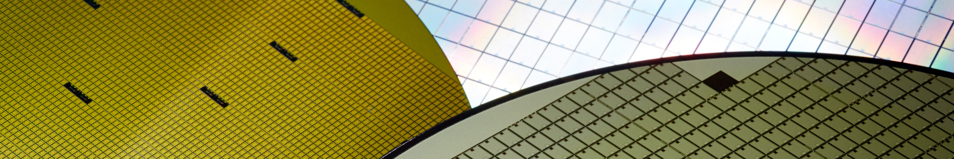
Semiconductor manufacturers primarily sell packaged parts with only a fraction of their production sold as bare die. The manufacturing process is geared toward packaged parts and die sales are frequently viewed as a nuisance. The manufacturer produces boats of wafers that can yield various device types. The wafers are probed to verify process control and to be sure minimal performance levels will be met. Individual dice are then separated off of the wafer, packaged and sent through Automated Test Equipment (ATE) which sorts them into different part numbers based on their electrical performance. Through this process, the yield from a wafer is maximized and numerous devices can be offered for sale. Products to be sold as bare die only complete part of this process. They are removed from the flow after wafer probe and are sent to the die distributor at that point. The probe process is only capable of accurately measuring a few DC parameters on a device. Additional probing can be done by the distributor, but it will still only measure DC parameters and it will cause additional damage to the die bond pads. Dice are not routinely tested over temperature or burned-in unless it is required by the specific end customer.
Die distributors frequently package samples from a die lot to facilitate Lot Acceptance Testing (LAT). Additional electrical testing of each device in a lot can be accomplished through various Known Good Die (KGD) techniques. The cost of this testing is prohibitive in many applications and the performance of DC probed die is often sufficient to meet circuit requirements. KGD is emerging technology with many methods, opinions and issues which are too involved to cover in this guide.
Visual inspection becomes far more important when using bare die since less electrical testing is done. It is assumed that die which look perfect will perform well. Die distributors are experts at visual inspection with their intimate knowledge of the military specifications for die inspection. The current version of the die geometry must be obtained and the propensity for the geometry to be changed or shrunk must be considered by the die user. Manufacturers will incorporate a die shrink to increase the number of devices that they can yield from a wafer. This has no effect on packaged product users who are unaware of any change to the die inside their packages. Bare die users can be adversely affected by such a change. A franchised die distributor will be provided with process change notification from its suppliers. News of a pending geometry change or other process variation will be passed along to the die user in advance of the change.
Once devices that are available in die form have been identified, samples will probably be needed to prove out the design. A franchised die distributor will be able to provide samples and data on most devices although it is not always possible to get samples on every device. Since manufacturers sell such a small percentage of their products as die, they do not always have small quantities available for sampling. Often, part types that are routinely sold in packaged form are not even offered as bare die. If a manufacturer agrees to offer a device as bare die, the minimum buy quantity is often much higher than the customer requires.
Most designers assume that all devices that a manufacturer sells in packages are available to purchase as die. While it is true that they must produce the die to offer it in a package, it is not true that everything is available as bare die. To be cost effective, most of the semiconductor manufacturing process is automated. Wafers get probed, diced, packaged and tested in rapid succession. It is not a simple thing to remove a wafer form this flow and manufacturers do not like to do it. Typically, devices are offered in bare die form only if the demand is high. If a device is not offered, it may be possible to get it added if the volumes are sufficient.
Franchised die distributors exist to minimize the headaches for manufacturers and die users alike. By identifying high volume parts, purchasing in wafer quantities, dicing wafers, performing visual inspection/electrical testing and stocking products in die form, they enable circuit builders to realize the advantages that bare die offer. To view frequently asked questions, click on this link to go to our FAQ page.